

– LaserFocusWorld

 In the News
  April 3, 2023
⚠️ Website Under Construction
In the News
April 3, 2023
– LaserFocusWorld
 In the News
April 3, 2023
In the News
April 3, 2023
– LightwaveOnline
 Press Releases
March 27, 2023
Press Releases
March 27, 2023
EFFECT Photonics is delighted to announce that it is on the list of 50 most…
EFFECT Photonics is delighted to announce that it is on the list of 50 most promising European Deep Tech start-ups as part of the EIC ScalingUp programme. A Selection Committee of experienced investors chose to include EFFECT Photonics from more than 3,000 candidates in a selection process covering several stages. These companies are considered the most promising EIC (European Innovation Council) deep tech companies that have the potential to achieve substantial growth, and to become world-scale companies or to realise a big exit or IPO.
“Through the EIC ScalingUp project the EIC supports high-growth, high potential companies with visionary ideas, disruptive technologies, and the ambition to grow exponentially in Europe and globally.”– Jean-David Malo, Director, European Innovation Council (EIC) and SMEs Executive Agency (EISMEA).
“We are honoured to be part of this select group. Our thanks go to the European Innovation Council, Tech Tour, DeepWave Ventures, Boston Consulting Group and bpifrance for the opportunity to further expand on our ambitions to make complex, powerful optical systems simpler and more accessible.”– James Regan, CEO EFFEFCT Photonics.
To learn more about the EIC ScalingUp programme, please click here.
To download the Top50 Publication, please click here.
About EFFECT Photonics
EFFECT Photonics delivers highly integrated optical communications products based on its Dense Wavelength Division Multiplexing (DWDM) optical System-on-Chip technology. The key enabling technology for DWDM systems is full monolithic integration of all photonic components within a single chip and being able to produce these in volume with high yield at low cost. With this capability, EFFECT Photonics is addressing the need for low cost DWDM solutions driven by the soaring demand for high bandwidth connections. EFFECT Photonics is headquartered in Eindhoven, The Netherlands, with additional R&D and manufacturing in South West UK, a subsidiary in Taiwan, a facility opening shortly outside Boston, and a worldwide network of sales partners.

 Press Releases
March 27, 2023
Press Releases
March 27, 2023
EFFECT Photonics is pleased to share that it has been chosen as one of the…
EFFECT Photonics is pleased to share that it has been chosen as one of the 2021 Deep Tech Programme winners.
EFFECT Photonics was one of the 46 selected companies, from a pool of over 300 candidates, presenting their business at the TechTour Deep Tech Programme 2021 (https://techtour.com) on 17-18 November 2021. The main goal was to unite the top deep tech companies in seeking funding with 200+ corporate and VC investors during a focused 2-day online event.

About EFFECT Photonics
For further information please contact sales@effectphotonics.com
EFFECT Photonics delivers highly integrated optical communications products based on its Dense Wavelength Division Multiplexing (DWDM) optical System-on-Chip technology. The key enabling technology for DWDM systems is full monolithic integration of all photonic components within a single chip and being able to produce these in volume with high yield at low cost. With this capability, EFFECT Photonics is addressing the need for low cost DWDM solutions driven by the soaring demand for high bandwidth connections between datacentres and back from mobile cell towers. EFFECT Photonics is headquartered in Eindhoven, The Netherlands, with additional R&D and manufacturing in South West UK, a facility opening soon in the Greater Boston Area and sales partners worldwide. www.effectphotonics.com
Tags: Deep Tech, EFFECT Photonics, Photonics, transceiversSFP Press Releases
March 27, 2023
Press Releases
March 27, 2023
NASA’s Jet Propulsion Laboratory lists EFFECT Photonics and its powerful monolithically integrated PIC (Photonic Integrated…
NASA’s Jet Propulsion Laboratory lists EFFECT Photonics and its powerful monolithically integrated PIC (Photonic Integrated Circuit) DWDM optical transceiver chip, as an example of State-of-Art commercial PIC. Packaging PIC’s for space applications remains a challenge. EFFECT Photonics has specially developed non-hermetic packaging solution, which can be used to replace traditional ”gold-box” packaging solutions. According to NASA optical communications is the future of space communications and the driving force is the requirement for more bandwidth, which is available only using optical solutions such as free-space laser links in both inter-satellite and satellite-to-ground communications.

EFFECT Photonics’ System-on-Chip (SoC)
EFFECT Photonics is the first company in the world to introduce a full optical SoC – combining all the optical elements needed for optical networking onto a single die.
One key application of EFFECT Photonics’ SoC technology is within dense wavelength division multiplexing (DWDM), and this is regarded as an important innovation in optical networks. DWDM is scalable, transparent and enables provision of high-bandwidth services. It is the technology of choice for many networking applications today. By using many different wavelengths of light to route data, these systems are more efficient, flexible, and cost-effective to build, own and operate compared to single-channel, point-to-point links. Thanks to our high-density electrical interconnect and packaging technology, the optical system-on-a-chip can be assembled for volume manufacture at low cost.
As the channel count increases, the physical space in which the equipment is housed gets larger and the power consumption increases as well. The key enablers for DWDM systems at the edge of the network are photonic integration of components within a single chip; and the ability to produce these in volume with high yield at low cost. This requires a change in the way indium phosphide (InP) chips are designed, tested, and packaged, which is where EFFECT Photonics comes in.
For further information about our products and technologies please visit our website www.effectphotonics.com or contact sales@effectphotonics.com
– About EFFECT Photonics –
EFFECT Photonics delivers highly integrated optical communications products based on its Dense Wavelength Division Multiplexing (DWDM) optical System-on-Chip technology. The key enabling technology for DWDM systems is full monolithic integration of all photonic components within a single chip and being able to produce these in volume with high yield at low cost. With this capability, EFFECT Photonics is addressing the need for low cost DWDM solutions driven by the soaring demand for high bandwidth connections between datacenters and back from mobile cell towers. Headquartered in Eindhoven, The Netherlands, with additional R&D and manufacturing in South West UK, with sales partners worldwide. www.effectphotonics.com
Tags: EFFECT Photonics, NASA, Photonics, PIC, Telecom, Transceivers Press Releases
March 27, 2023
Press Releases
March 27, 2023
EFFECT Photonics, a leading developer of high-performance dense wavelength division multiplexing (DWDM) optical components based…
EFFECT Photonics, a leading developer of high-performance dense wavelength division multiplexing (DWDM) optical components based on its optical System-on-Chip technology, has been selected as one of Europe’s 40 top high-tech startups to pitch at the High Tech Venture Days (HTVD) 2020. HTVD is one of Europe’s leading meeting places for tech companies, international investors and corporates and is launching on October 13-14 in Dresden, Germany.
Our CEO, James Regan, will be taking the stage at pitches and panel discussions and will give insight into the EFFECT Photonics’ unique integrated photonics technology. EFFECT Photonics is the first company in the world to introduce a full optical system-on-chip (SoC) – combining all the optical elements needed for optical networking onto a single die. One key application of EFFECT Photonics’ SoC technology is within dense wavelength division multiplexing (DWDM), and this is regarded as an important innovation in optical networks. DWDM is scalable, transparent and enables provision of high-bandwidth services. It is the technology of choice for many networking applications today. By using many different wavelengths of light to route data, these systems are more efficient, flexible, and cost-effective to build, own and operate compared to single-channel, point-to-point links. Thanks to our high-density electrical interconnect and packaging technology, the optical system-on-a-chip can be assembled for volume manufacture at low cost.
Let us talk at HTVD20, we will show how EFFECT Photonics will revolutionize the integrated photonics market with our Optical SoC technology.
For more on our technology, visit: https://old.effect.jkc-dev.nl/technology/
Get in touch with us for further information by sending your request to: sales@effectphotonics.com
Tags: DWDM, Hightech, HTVD, Photonics Insights
March 22, 2023
Insights
March 22, 2023
Artificial intelligence (AI) will have a significant role in making optical networks more scalable, affordable,…
Artificial intelligence (AI) will have a significant role in making optical networks more scalable, affordable, and sustainable. It can gather information from devices across the optical network to identify patterns and make decisions independently without human input. By synergizing with other technologies, such as network function virtualization (NFV), AI can become a centralized management and orchestration network layer. Such a setup can fully automate network provisioning, diagnostics, and management, as shown in the diagram below.
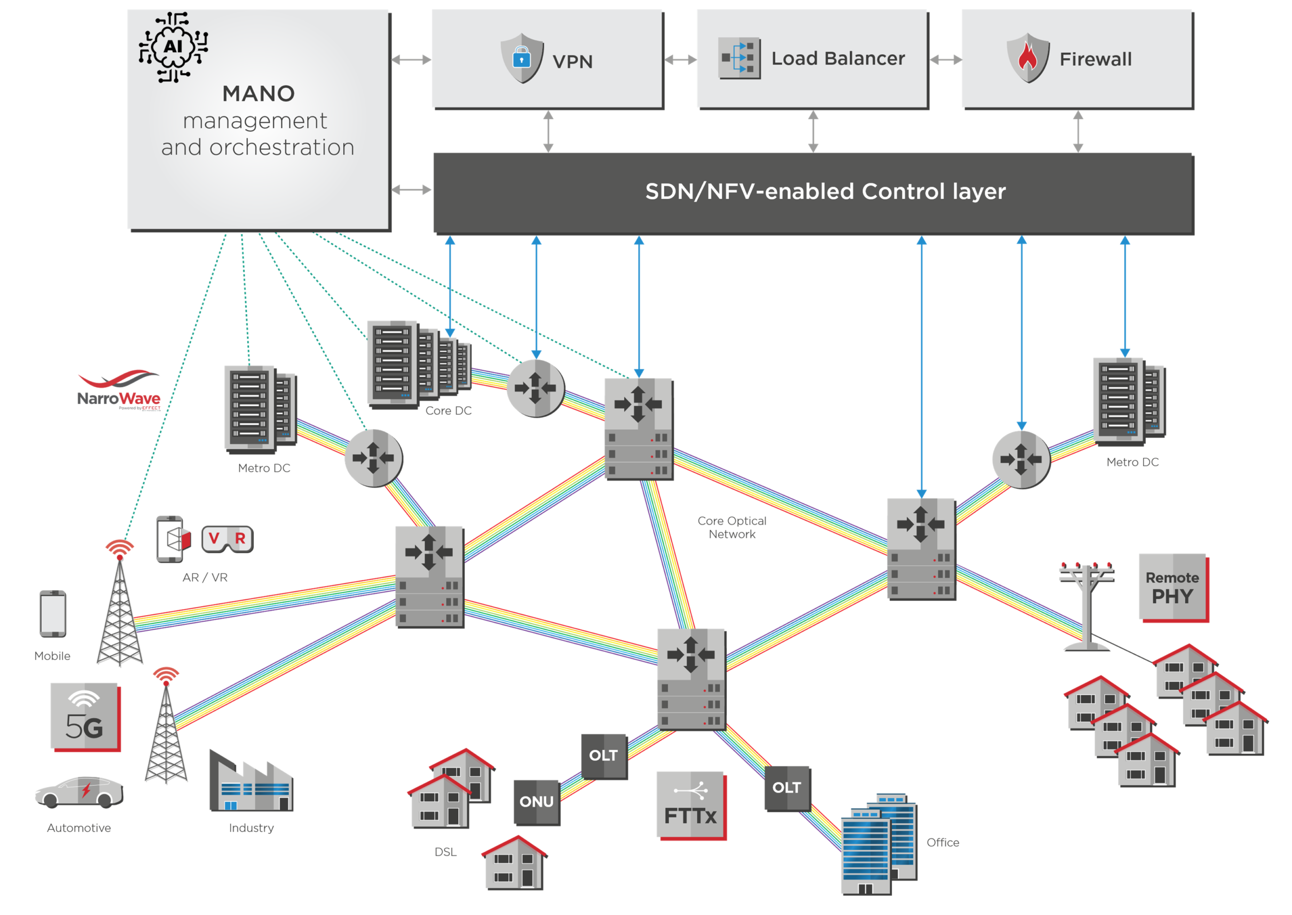
However, artificial intelligence and machine learning algorithms are data-hungry. To work optimally, they need information from all network layers and ever-faster data centers to process it quickly. Pluggable optical transceivers thus need to become smarter, relaying more information back to the AI central unit, and faster, enabling increased AI processing.
Optical transceivers are crucial in developing better AI systems by facilitating the rapid, reliable data transmission these systems need to do their jobs. High-speed, high-bandwidth connections are essential to interconnect data centers and supercomputers that host AI systems and allow them to analyze a massive volume of data.
In addition, optical transceivers are essential for facilitating the development of artificial intelligence-based edge computing, which entails relocating compute resources to the network’s periphery. This is essential for facilitating the quick processing of data from Internet-of-Things (IoT) devices like sensors and cameras, which helps minimize latency and increase reaction times.
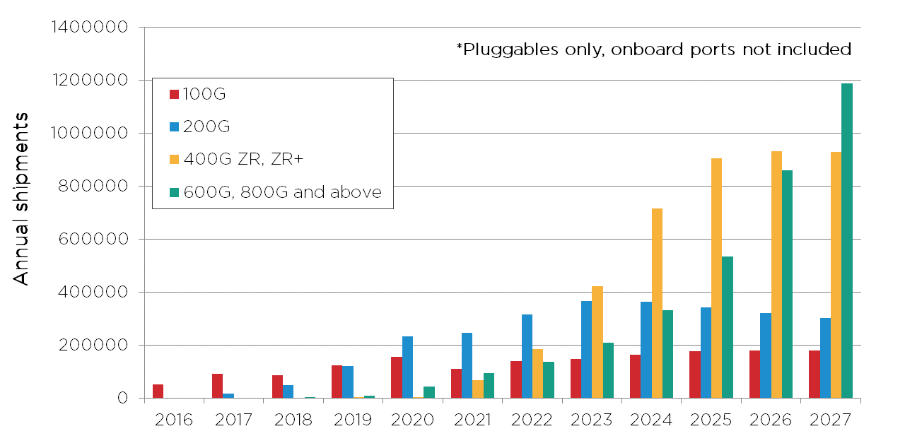
400 Gbps links are becoming the standard across data center interconnects, but providers are already considering the next steps. LightCounting forecasts significant growth in the shipments of dense-wavelength division multiplexing (DWDM) ports with data rates of 600G, 800G, and beyond in the next five years. We discuss these solutions in greater detail in our article about the roadmap to 800G and beyond.
Mobile networks now and in the future will consist of a massive number of devices, software applications, and technologies. Self-managed, zero-touch automated networks will be required to handle all these new devices and use cases. Realizing this full network automation requires two vital components.
These goals require smart optical equipment and components that provide comprehensive telemetry data about their status and the fiber they are connected to. The AI-controlled centralized management and orchestration layer can then use this data for remote management and diagnostics. We discuss this topic further in our previous article on remote provisioning, diagnostics, and management.
For example, a smart optical transceiver that fits this centralized AI-management model should relay data to the AI controller about fiber conditions. Such monitoring is not just limited to finding major faults or cuts in the fiber but also smaller degradations or delays in the fiber that stem from age, increased stress in the link due to increased traffic, and nonlinear optical effects. A transceiver that could relay all this data allows the AI controller to make better decisions about how to route traffic through the network.
After relaying data to the AI management system, a smart pluggable transceiver must also switch parameters to adapt to different use cases and instructions given by the controller.
Let’s look at an example of forward error correction (FEC). FEC makes the coherent link much more tolerant to noise than a direct detect system and enables much longer reach and higher capacity. In other words, FEC algorithms allow the DSP to enhance the link performance without changing the hardware. This enhancement is analogous to imaging cameras: image processing algorithms allow the lenses inside your phone camera to produce a higher-quality image.
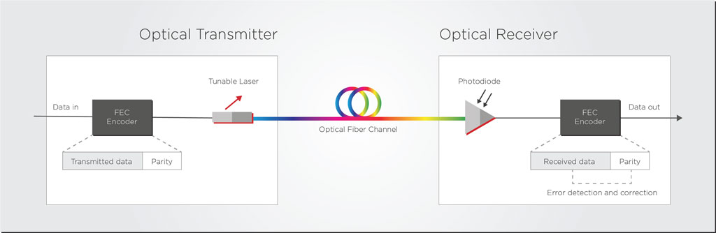
A smart transceiver and DSP could switch among different FEC algorithms to adapt to network performance and use cases. Let’s look at the case of upgrading a long metro link of 650km running at 100 Gbps with open FEC. The operator needs to increase that link capacity to 400 Gbps, but open FEC could struggle to provide the necessary link performance. However, if the transceiver can be remotely reconfigured to use a proprietary FEC standard, the transceiver will be able to handle this upgraded link.
Reconfigurable transceivers can also be beneficial to auto-configure links to deal with specific network conditions, especially in brownfield links. Let’s return to the fiber monitoring subject we discussed in the previous section. A transceiver can change its modulation scheme or lower the power of its semiconductor optical amplifier (SOA) if telemetry data indicates a good quality fiber. Conversely, if the fiber quality is poor, the transceiver can transmit with a more limited modulation scheme or higher power to reduce bit errors. If the smart pluggable detects that the fiber length is relatively short, the laser transmitter power or the DSP power consumption could be scaled down to save energy.
Optical networks will need artificial intelligence and machine learning to scale more efficiently and affordably to handle the increased traffic and connected devices. Conversely, AI systems will also need faster pluggables than before to acquire data and make decisions more quickly. Pluggables that fit this new AI era must be fast, smart, and adapt to multiple use cases and conditions. They will need to scale up to speeds beyond 400G and relay monitoring data back to the AI management layer in the central office. The AI management layer can then program transceiver interfaces from this telemetry data to change parameters and optimize the network.
Tags: 800G, 800G and beyond, adaptation, affordable, AI, artificial intelligence, automation, CloudComputing, data, DataCenter, EFFECT Photonics, FEC, fiber quality, innovation, integration, laser arrays, machine learning, network conditions, network optimization, Networking, optical transceivers, photonic integration, Photonics, physical layer, programmable interface, scalable, sensor data flow, technology, Telecommunications, telemetry data, terabyte, upgrade, virtualization 07 March 2023 - 09 March 2023
 8:00 am - 5:00 pm
 EFFECT Photonics #2423
Join EFFECT Photonics from March 7 to 9, 2023 at OFC in San Diego, California, the world’s largest event for optical networking and communications, to discover firsthand how our technology is transforming where light meets digital. Visit Booth #2423 to learn how EFFECT Photonics’ full portfolio of optical building blocks are enabling 100G coherent to the network edge and next-generation applications.
Build Your Own 100G ZR Coherent Module
At this year’s OFC, see how easy and affordable it can be to upgrade existing 10G links to a more scalable 100G coherent solution! Try your hand at constructing a 100G ZR coherent module specifically designed for the network edge utilizing various optical building blocks including tunable lasers, DSPs and optical subassemblies.
Tune Your Own PIC (Photonic Integrated Circuit)
Be sure to stop by Booth #2423 to tune your own PIC with EFFECT Photonics technology. In this interactive and dynamic demonstration, participants can explore first-hand the power of EFFECT Photonics solutions utilizing various parameters and product configurations.
Our experts are also available to discuss customer needs and how EFFECT Photonics might be able to assist. To schedule a meeting, please email marketing@effectphotonics.com
Tags: 100 ZR, 100G, 100gcoherent, access, access networks, bringing100Gtoedge, cloud, cloudedge, coherent, coherentoptics, datacenters, DSP, DSPs, EFFECT Photonics, Integrated Photonics, networkedge, ofc23, opticcommunications, Optics, photonic integration, Photonics, PIC, tunablelasers, wherelightmeetsdigital Insights
February 7, 2023
Insights
February 7, 2023
When it started, the space race was a competition between two superpowers, but now there…
When it started, the space race was a competition between two superpowers, but now there are 90 countries with missions in space.
The prices of space travel have gone down, making it possible for more than just governments to send rockets and satellites into space. Several private companies are now investing in space programs, looking for everything from scientific advances to business opportunities. Some reports estimate more than 10,000 companies in the space industry and around 5,000 investors.
According to The Space Foundation’s 2022 report, the space economy was worth $469 billion in 2021. The report says more spacecraft were launched in the first six months of 2021 than in the first 52 years of space exploration (1957-2009). This growing industry has thus a growing need for technology products across many disciplines, including telecommunications. The space sector will need lighter, more affordable telecommunication systems that also provide increased bandwidth.
This is why EFFECT Photonics sees future opportunities for coherent technology in the space industry. By translating the coherent transmission from fiber communication systems on the ground to free-space optical systems, the space sector can benefit from solutions with more bandwidth capacity and less power consumption than traditional point-to-point microwave links.
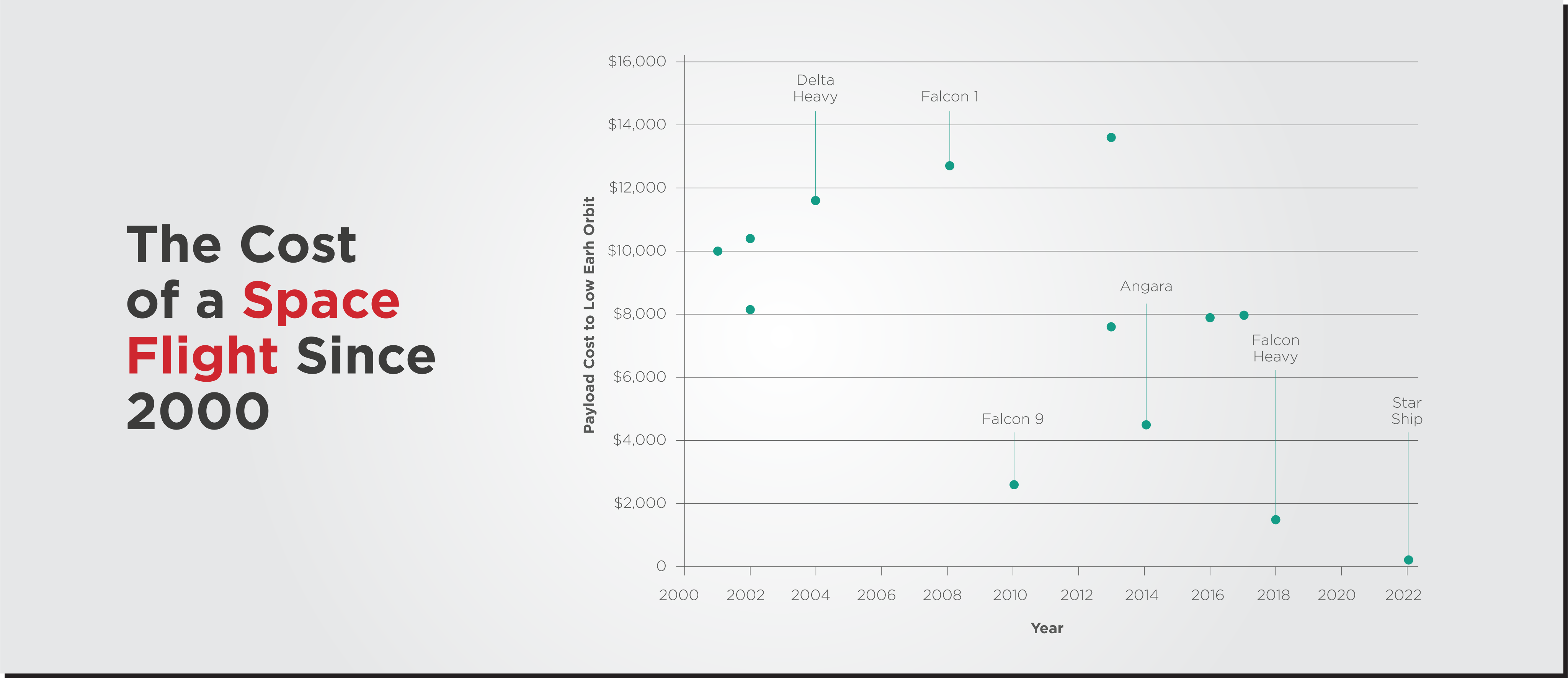
One of the major concerns of the space industry is the cost of sending anything into space. Even during the days of NASA’s Space Shuttle program (which featured a reusable shuttle unit), sending a kilogram into space cost tens of thousands of dollars. Over time, more rocket stages have become reusable due to the efforts of companies like SpaceX, reducing these costs to just a few thousand. The figure below shows how the cost of space flight has decreased significantly in the last two decades.
Even though space travel is more affordable than ever, size, weight, and power (SWaP) requirements are still vital in the space industry. After all, shaving off weight or size in the spacecraft means a less expensive launch or perhaps room for more scientific instruments. Meanwhile, less power consumption means less drain on the spacecraft’s energy sources.
Currently, most space missions use bulkier radio frequency communications to send data to and from spacecraft. While radio waves have a proven track record of success in space missions, generating and collecting more mission data requires enhanced communications capabilities. Besides, radiofrequency equipment can often generate a lot of heat, requiring more energy to cool the system.
Decreasing SWaP requirements can be achieved with more photonics and miniaturization. Transmitting data with light will usually dissipate less than heat than transmission with electrical signals and radio waves. These leads to smaller, lighter communication systems that require less power to run.
These SWaP advantages come alongside the increased transmission speeds. After all, coherent optical communications can increase link capacities to spacecraft and satellites by 10 to 100 times that of radio frequency systems.
While integrated photonics can boost space communications by lowering the payload, it must overcome the obstacles of a harsh space environment, which include radiation hardness, an extreme operational temperature range, and vacuum conditions.
| Mission Type | Temperature Range |
|---|---|
| Pressurized Module | +18.3 ºC to 26.7 °C |
| Low-Earth Orbit (LEO) | -65 ºC to +125 °C |
| Geosynchronous Equatorial Orbit (GEO) | -196 ºC to +128 °C |
| Trans-Atmospheric Vehicle | -200 ºC to +260 ºC |
| Lunar Surface | -171 ºC to +111 ºC |
| Martian Surface | -143 ºC to +27 ºC |
The values in Table 1 show the unmanaged environmental temperatures in different space environments. In a temperature-managed area, these would decrease significantly for electronics and optics systems, perhaps by as much as half. Despite this management, the equipment would still need to deal with some extreme temperature values.
Fortunately, a substantial body of knowledge exists to make integrated photonics compatible with space environments. After all, photonic integrated circuits (PICs) use similar materials to their electronic counterparts, which have already been space qualified in many implementations.
Much research has gone into overcoming the challenges of packaging PICs with electronics and optical fibers for these space environments, which must include hermetic seals and avoid epoxies. Commercial solutions, such as those offered by PHIX Photonics Assembly, Technobis IPS, and the PIXAPP Photonic Packaging Pilot Line, are now available.
Whenever you want to send data from point A to B, photonics is usually the most efficient way of doing it, be it over fiber or free space.
Offering optical communication systems in a small integrated package that can resist the required environmental conditions will significantly benefit the space sector and its need to minimize SWaP requirements. These optical systems can increase their transmission capacity with the coherent optical transmission used in fiber optics. Furthermore, by leveraging the assembly and packaging structure of electronics for the space sector, photonics can also provide the systems with the ruggedness required to live in space.
Tags: certification, coherent, electronics, existing, fast, growing, heat dissipation, miniaturization, Optical Communication, Photonics, power consumption, size, space, space sector, speed, SWAP, temperature, weight Insights
December 9, 2022
Insights
December 9, 2022
Over the last two decades, power ratings for pluggable modules have increased as we moved…
Over the last two decades, power ratings for pluggable modules have increased as we moved from direct detection to more power-hungry coherent transmission: from 2W for SFP modules to 3.5 W for QSFP modules and now to 14W for QSSFP-DD and 21.1W for OSFP form factors. Rockley Photonics researchers estimate that a future electronic switch filled with 800G modules would draw around 1 kW of power just for the optical modules.
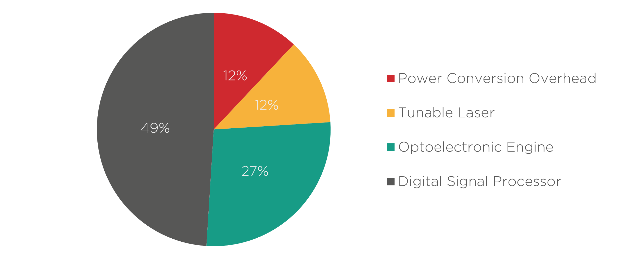
Around 50% of a coherent transceiver’s power consumption goes into the digital signal processing (DSP) chip that also performs the functions of clock data recovery (CDR), optical-electrical gear-boxing, and lane switching. Scaling to higher bandwidths leads to even more losses and energy consumption from the DSP chip and its radiofrequency (RF) interconnects with the optical engine.
One way to reduce transceiver power consumption requires designing DSPs that take advantage of the material platform of their optical engine. In this article, we will elaborate on what that means for the Indium Phosphide platform.
Transceiver developers often source their DSP, laser, and optical engine from different suppliers, so all these chips are designed separately from each other. This setup reduces the time to market and simplifies the research and design processes but comes with trade-offs in performance and power consumption.
In such cases, the DSP is like a Swiss army knife: a jack of all trades designed for different kinds of optical engines but a master of none. For example, current DSPs are designed to be agnostic to the material platform of the photonic integrated circuit (PIC) they are connected to, which can be Indium Phosphide (InP) or Silicon. Thus, they do not exploit the intrinsic advantages of these material platforms. Co-designing the DSP chip alongside the PIC can lead to a much better fit between these components.
To illustrate the impact of co-designing PIC and DSP, let’s look at an example. A PIC and a standard platform-agnostic DSP typically operate with signals of differing intensities, so they need some RF analog electronic components to “talk” to each other. This signal power conversion overhead constitutes roughly 2-3 Watts or about 10-15% of transceiver power consumption.
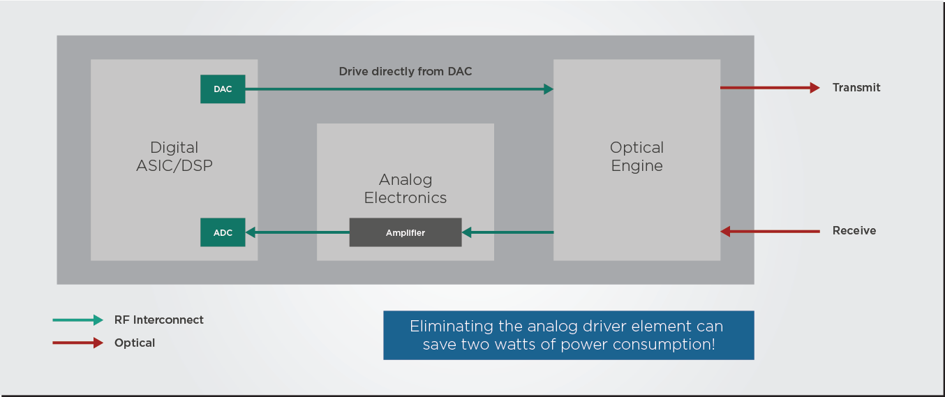
However, the modulator of an InP PIC can run at a lower voltage than a silicon modulator. If this InP PIC and the DSP are designed and optimized together instead of using a standard DSP, the PIC could be designed to run at a voltage compatible with the DSP’s signal output. This way, the optimized DSP could drive the PIC directly without needing the RF analog driver, doing away with most of the power conversion overhead we discussed previously.
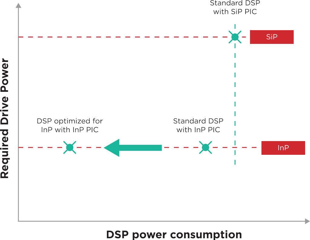
Additionally, the optimized DSP could also be programmed to do some additional signal conditioning that minimizes the nonlinear optical effects of the InP material, which can reduce noise and improve performance.
Russell Fuerst, EFFECT Photonics’ Vice-President of Digital Signal Processing, gave us an interesting insight about designing for the InP platform in a previous interview:
When we started doing coherent DSP designs for optical communication over a decade ago, we pulled many solutions from the RF wireless and satellite communications space into our initial designs. Still, we couldn’t bring all those solutions to the optical markets.
However, when you get more of the InP active components involved, some of those solutions can finally be brought over and utilized. They were not used before in our designs for silicon photonics because silicon is not an active medium and lacked the performance to exploit these advanced techniques.
For example, the fact that the DSP could control laser and modulator components on the InP can lead to some interesting manipulations of light signals. A DSP that can control these components directly could generate proprietary waveforms or use non-standard constellation and modulation schemes that can boost the performance of a coherent transceiver and increase the capacity of the link.
The biggest problem for DSP designers is still improving performance while reducing power use. This problem can be solved by finding ways to integrate the DSP more deeply with the InP platform, such as letting the DSP control the laser and modulator directly to develop new waveform shaping and modulation schemes. Because the InP platforms have active components, DSP designers can also import more solutions from the RF wireless space.
Tags: analog electronics, building blocks, coherent, dispersion compensation, DSP, energy efficiency, Intra DCI, Photonics, PON, power consumption, reach, simplified© 2026 EFFECT PHOTONICS All rights reserved. T&C of Website - T&C of Purchase - Privacy Policy - Cookie Policy - Supplier Code of Conduct