

– 거제인터넷방송 GİB

 In the News
  October 6, 2023
⚠️ Website Under Construction
In the News
October 6, 2023
– 거제인터넷방송 GİB
 In the News
October 6, 2023
In the News
October 6, 2023
– SemiconductorToday
 In the News
October 6, 2023
In the News
October 6, 2023
– optics.org
 02 October 2023 - 04 October 2023
 9:30 am - 4:30 pm
 EFFECT Photonics #547
Join EFFECT Photonics from October 2nd-4th, 2023 at ECOC Exhibition in Sec, Glasgow, Scotland. ECOC is the largest optical communications exhibition in Europe and a key meeting place for decision-makers. Come and discover firsthand how our technology is transforming where light meets digital, visit booth #547 to learn how EFFECT Photonics’ full portfolio of optical building blocks are enabling 100G coherent to the network edge and next-generation applications.
Build Your Own 100G ZR Coherent Module
At this year’s ECOC, see how easy and affordable it can be to upgrade existing 10G links to a more scalable 100G coherent solution! Try your hand at constructing a 100G ZR coherent module specifically designed for the network edge utilizing various optical building blocks including tunable lasers, DSPs and optical subassemblies.
Tune Your Own PIC (Photonic Integrated Circuit)
Be sure to stop by stand #547 to tune your own PIC with EFFECT Photonics technology. In this interactive and dynamic demonstration, participants can explore first-hand the power of EFFECT Photonics solutions utilizing various parameters and product configurations.
Our experts are also available to discuss customer needs and how EFFECT Photonics might be able to assist. To schedule a meeting, please email marketing@effectphotonics.com
Tags: 100 ZR, 100G, 100gcoherent, access, access networks, bringing100Gtoedge, cloud, cloudedge, coherent, coherentoptics, datacenters, DSP, DSPs, ECOC, ECOC2023, EFFECT Photonics, Integrated Photonics, networkedge, opticcommunications, Optics, photonic integration, Photonics, PIC, tunablelasers, wherelightmeetsdigital Insights
July 28, 2023
Insights
July 28, 2023
Last year, EFFECT Photonics announced the acquisition of the coherent optical digital signal processing (DSP)…
Last year, EFFECT Photonics announced the acquisition of the coherent optical digital signal processing (DSP) and forward error correction (FEC) business unit from the global communications company Viasat Inc. This also meant welcoming to the EFFECT Photonics family a new engineering team who will continue to work in the Cleveland area.
As EFFECT Photonics expands its influence into the American Midwest, it is interesting to dive deeper into Cleveland’s history with industry and technology. Cleveland has enjoyed a long story as a Midwest industrial hub, and as these traditional industries have declined, it is evolving into one of the high-tech hubs of the region.
Cleveland’s industrial sector expanded significantly in the 19th century because of the city’s proximity to several essential resources and transportation routes: coal and iron ore deposits, the Ohio and Erie Canal, and the Lake Erie railroad. For example, several steel mills, such as the Cleveland Rolling Mill Company and the Cleveland Iron and Steel Company, emerged because of the city’s proximity to Lake Erie, facilitating the transportation of raw materials and goods.
Building on the emerging iron and steel industries, heavy equipment production also found a home in Cleveland. Steam engines, railroad equipment, and other forms of heavy machinery were all manufactured in great quantities in the city.

Cleveland saw another massive boost to its industrial hub status with the birth of the Standard Oil Company in 1870. At the peak of its power, Standard Oil was the largest petroleum company in the world, and its success made its founder and head, John D. Rockefeller, one of the wealthiest men of all time. This history with petroleum also led to the emergence of Cleveland’s chemicals and materials industry.
Many immigrants moved to Cleveland, searching for work in these expanding industries, contributing to the city’s rapid population boom. This growth also prompted the development of new infrastructure like roads, railways and bridges to accommodate the influx of people.
Several important electrical and mechanical equipment manufacturers, including the Bendix Corporation, the White Motor Company, and the Western Electric Company (which supplied equipment to the US Bell System), also established their headquarters in or around Cleveland in the late 19th and early 20th century.
In the second half of the 20th century, Cleveland’s traditional industries, such as steel and manufacturing in Cleveland began to collapse. As was the case in many other great American manufacturing centers, automation, globalization, and other socioeconomic shifts all had a role in this decline. The demise of Cleveland’s core industries was a significant setback, but the city has made substantial efforts in recent years to diversify its economy and grow in new technology and healthcare areas.
For example, the Cleveland Clinic is one of the leading US academic medical centers, with pioneering medical breakthroughs such as the first coronary artery bypass surgery and the first face transplant in the United States. Institutions like theirs or the University Hospitals help establish Cleveland as a center for healthcare innovation.
Cleveland is also trying to evolve as a high-tech hub that attracts new workers and companies, especially in software development. Companies are attracted by the low office leasing and other operating costs, while the affordable living costs attract workers. As reported by the real estate firm CBRE, Cleveland’s tech workforce grew by 25 percent between 2016 and 2021, which was significantly above the national average of 12.8 percent.
As Cleveland’s history as a tech hub continues, EFFECT Photonics is excited to join this emerging tech environment. Our new DSP team will find its new home in the Wagner Awning building in the Tremont neighborhood of Cleveland’s West Side.

This building was erected in 1895 and hosted a sewing factory that manufactured everything from tents and flotation devices for American soldiers and marines to awnings for Cleveland buildings. When the Ohio Awning company announced its relocation in 2015, this historic building began a redevelopment process to become a new office and apartment space.
EFFECT Photonics is proud to become a part of Cleveland’s rich and varied history with industry and technology. We hope our work can help develop this city further as a tech hub and attract more innovators and inventors to Cleveland.
Tags: digital signal processing (DSP), EFFECT Photonics, forward error correction (FEC), high-tech hub, industrial history, Integrated Photonics, Ohio Awning Company, Photonics, Tremont neighborhood, Viasat Inc., Wagner Awning building Insights
July 28, 2023
Insights
July 28, 2023
As they lighted the candles in their ship, the Pilgrim families traveling on the Mayflower had no…
As they lighted the candles in their ship, the Pilgrim families traveling on the Mayflower had no idea they would help build a nation that would become a major pioneer in light technology and many other fields.
The United States features many areas with a strong photonics background, including the many companies in California’s Silicon Valley and the regions close to the country’s leading optics universities, such as Colorado, New York, Arizona, and Florida.
However, the Greater Boston area and Massachusetts state, in general, are becoming an increasingly important photonics hub with world-class universities and many successful optics and photonics initiatives and companies. Let’s talk a bit more about their legacy with light-based technology and the history of the town of Maynard with the high-tech industry.
The Boston area features many world-class universities collaborating with the government and industry to develop new photonics technology. Harvard, the Massachusetts Institute of Technology (MIT), Boston University, Tufts University, and Northeastern University are major research institutions in the area that lead many photonics-related initiatives.

The state of Massachusetts, in general, has also been home to several prosperous photonics businesses, and initiatives are being made to capitalize on Boston’s extensive medical industry knowledge to boost biomedical optics and photonics. Raytheon, Polaroid, and IPG Photonics are examples of Massachusetts-based businesses that promoted optical technology.
The US federal government and Massachusetts state are committing resources to get these academic and industry partners to collaborate as much as possible. In 2015, the Lab for Education and Application Prototypes (LEAP) network was established as part of a federal drive to revive American manufacturing. The Massachusetts Manufacturing Innovation Initiative, a state grant program, and AIM Photonics, the national manufacturing institution, each contributed $11.3 million to constructing labs around Massachusetts universities and colleges.
The LEAP Network objectives are to teach integrated photonics manufacturing practice, offer companies technician training and certification, encourage company engagement in the tool, process, and application upgrades, and support AIM Photonics in their manufacturing and testing.
These partnerships form a statewide ecosystem to educate the manufacturing workforce throughout the photonics supply chain. The facilities’ strategic placement next to both universities and community colleges allows them to attract students from all areas and stages of their careers, from technicians to engineers to fundamental researchers.
A trip down Route 2 into Middlesex County, 25 miles northwest of Boston, will take one past apple orchards, vineyards, and some of Massachusetts’ most stunning nature preserves before arriving at a historic mill on the Assabet River. The community around this mill, Maynard, is a charming and surprisingly historical hub of economic innovation that houses an emerging tech ecosystem.

The renowned Assabet Woolen Mill was established for textile manufacturing in 1847 by Amory Maynard, who by the age of 16 was managing his own sawmill company. Initially a carpet manufacturing plant, Maynard’s enterprise produced blankets and uniforms for the Union Army during the Civil War. The company employed immigrants from Ireland, Finland, Poland, Russia, and Italy, many of them coming to the mill for jobs as soon as they arrived in the nation. By the 1930s, the town of Maynard was recognized as one of the most multi-ethnic places in the state.
The Assabet Woolen Mill continued to create textiles until 1950. The 11-acre former mill complex, currently named Mill and Main, is the contemporary expression of the town’s evolution and relationship with innovative industry.
The Digital Equipment Corporation (DEC) occupied the facility before the end of the 50s with just $70,000 cash and three engineers. From the 1960s onward, DEC became a major global supplier of computer systems and enjoyed tremendous growth. It’s hard to overstate the company’s impact on Maynard, which became the ” Mini Computer Capital of the World” in barely twenty years.
Following DEC’s departure, the mill complex was sold and rented out to a fresh group of young and ambitious computer startups, many of whom are still operating today. Since then, more people and companies have joined, noting the affordable real estate, the enjoyable commute and environs, and the obvious cluster of IT enterprises. For example, when Acacia Communications, Inc. was established in 2009 and needed a home, Maynard’s mill space was a natural fit.
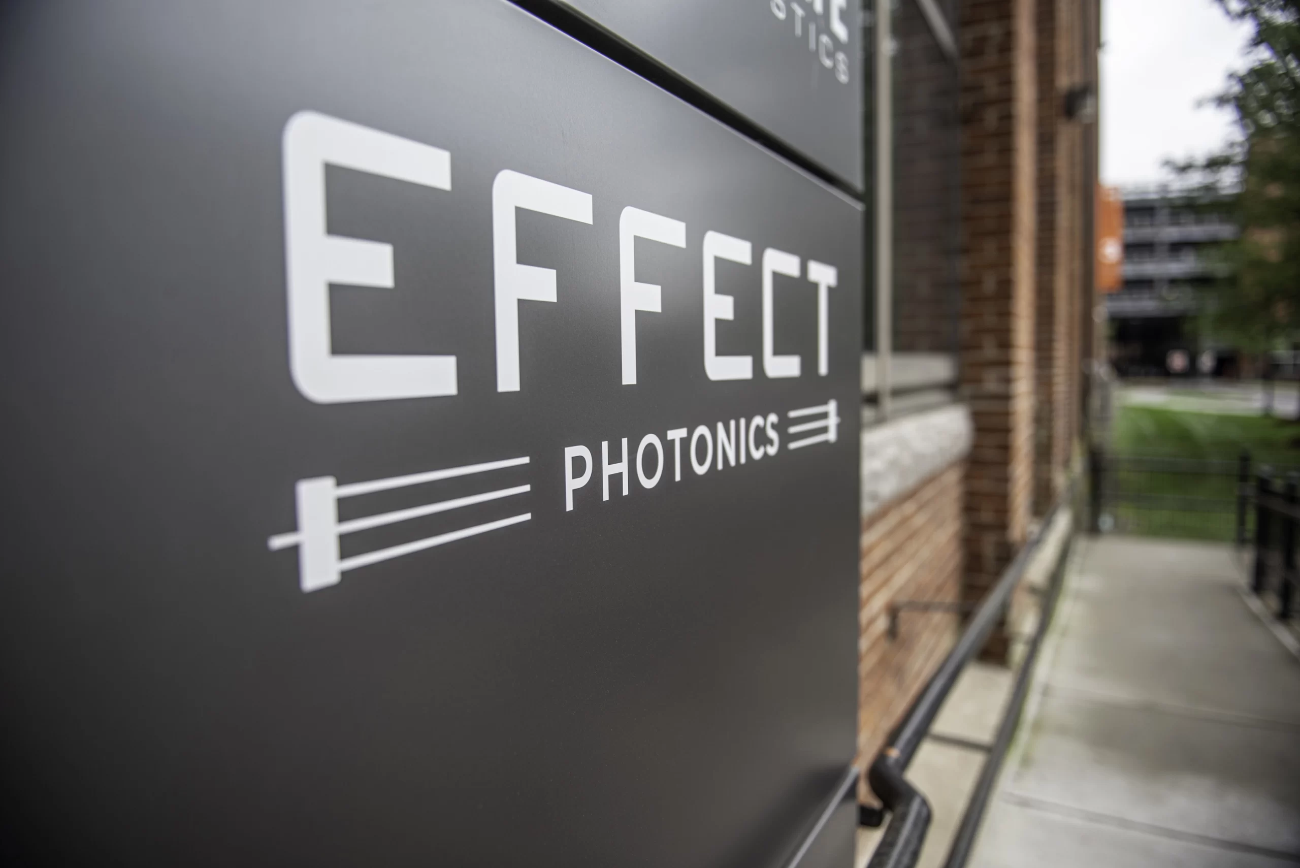
Similarly, EFFECT Photonics is proud to make a home in Maynard´s historic mill space and be a part of this community’s innovative heritage. We hope our work can serve as a positive example and inspiration for the neighborhood and help more innovators and inventors come to Maynard.
Tags: Boston, Boston University, DEC, Maynard, MIT, Photonics, Woolen Mill Insights
July 28, 2023
Insights
July 28, 2023
Paris may be the more well-known City of Light, but we may argue that Eindhoven…
Paris may be the more well-known City of Light, but we may argue that Eindhoven has had a closer association with light and light-based technology. The earliest Dutch match manufacturers, the Philips light bulb factory, and ASML’s enormous optical lithography systems were all located in Eindhoven during the course of the city’s 150-year history. And today, Eindhoven is one of the worldwide hubs of the emerging photonics industry. The heritage of Eindhoven’s light technology is one that EFFECT Photonics is honored to continue into the future.
Eindhoven’s nickname as the Lichtstad did not originate from Philips factories but from the city’s earlier involvement in producing lucifer friction matches. In 1870, banker Christiaan Mennen and his brother-in-law Everardus Keunen set up the first large-scale match factory in the Netherlands in Eindhoven’s Bergstraat. In the following decades, the Mennen & Keunen factory acquired other match factories, and promoted the merger of the four biggest factories in the country to form the Vereenigde Nederlandsche Lucifersfabriken (VNLF). After 1892, the other three factories shut down, and all the match production was focused on Eindhoven. Over the course of the next century, the Eindhoven match factory underwent a number of ownership and name changes until ceasing operations in 1979.
Two decades after the founding of the original match factory, businessman Gerard Philips bought a small plant at the Emmasingel in Eindhoven with the financial support of his father, Frederik, a banker. After a few years, Gerard’s brother Anton joined the company and helped it expand quickly. The company succeeded in its first three decades by focusing almost exclusively on a single product: metal-filament light bulbs.
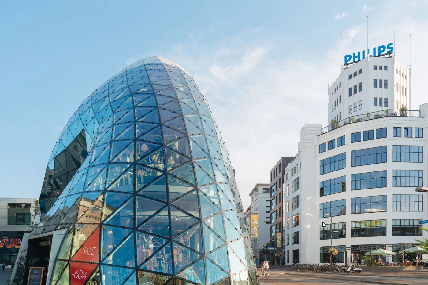
Over time, Philips began manufacturing various electro-technical products, including vacuum tubes, TVs, radios, and electric shavers. Philips was also one of the key companies that helped develop the audio cassette tape was Philips. In the 1960s, Philips joined the electronic revolution that swept the globe and proposed early iterations of the VCR cassette tape.
In 1997, Philips relocated their corporate headquarters outside of Eindhoven, leaving a significant void in the city. Philips was the primary factor in Eindhoven’s growth, attracting many people to the city to work.
Fortunately, Philips’ top-notch research and development led to several major spinoff companies, such as NXP and ASML. While ASML is already well-known across Eindhoven and is arguably the city’s largest employer, it might just be the most important tech company the world hasn’t heard of. In order to produce the world’s electronics, ASML builds enormous optical lithography systems that are shipped to the largest semiconductor facilities on earth. The scale of these systems requires engineers from all fields—electrical, optical, mechanical, and materials—to develop them, and that has attracted top talent from all over the world to Eindhoven. Thanks to their growth, Eindhoven has developed into a major center for expats in the Netherlands.

As ASML grew into a global powerhouse, the Eindhoven University of Technology (TU/e) worked tirelessly over the last 30 years to develop the light technology of the future: photonics. Photonics is used to create chips like the electronics inside your computers and phones, but instead of using electricity, these chips use laser light. Replacing electricity with light dramatically increases the speed of data transmission while also decreasing its power consumption. These benefits would lead photonics to have a significant impact in several industries, especially telecommunications.
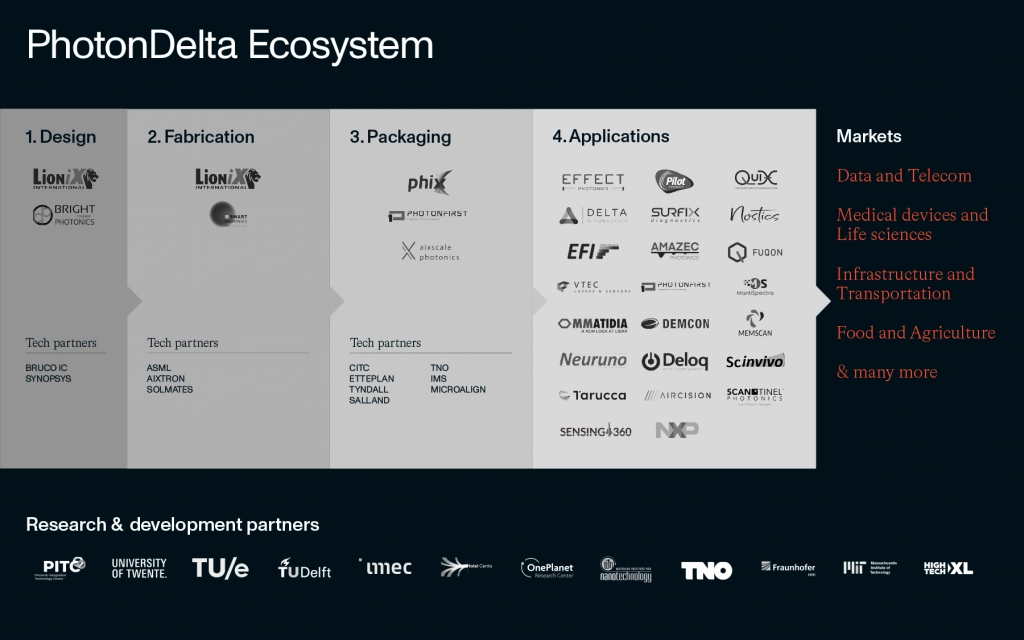
The photonics discoveries occurring in Eindhoven have been making strides in the lab for the last 30 years, and now they are finally becoming businesses. The founders of EFFECT Photonics were once TU/e students who wanted to take their lab research outside into the real world. Like us, there are many other companies in who are trying to bring new and exciting technologies into market, such as SMART Photonics (semiconductor manufacturing), Lightyear (solar electric cars), or Aircision (free space optics). Many of these companies have gathered in the High Tech Campus in Eindhoven and the PhotonDelta cluster, which gathers photonics companies in the Netherlands. The figure below provides a comprehensive picture of the entire PhotonDelta Ecosystem.
The TU/e environment has also championed processes that allow integrated photonics to become more widespread and easier to develop for market applications. The JePPIX consortium has aimed at creating a common platform of indium-phosphide chip design and manufacturing blocks that can become a “language” that every photonics developer in Europe can follow to make their devices. Meanwhile, photonics research and develop continues on many fronts, including biomedical devices, next-generation telecommunications, and improving photonics manufacturing’s compatibility with electronics. Hopefully, additional companies will emerge in the next years to bring these novel technologies to market.
As you can see, Eindhoven has a long history with light, from matches to light bulbs to TVs to optical lithography and photonics. The heritage of Eindhoven’s light technology is one that EFFECT Photonics is honored to carry into the future.
Tags: 5G, access, aggregation, backhaul, capacity, DWDM, fronthaul, Integrated Photonics, LightCounting, metro, midhaul, mobile, mobile access, network, optical networking, optical technology, photonic integrated chip, photonic integration, Photonics, PIC, PON, programmable photonic system-on-chip, solutions, technology Insights
July 27, 2023
Insights
July 27, 2023
On October 21st, 1983, the General Conference of Weights and Measures adopted the current value…
On October 21st, 1983, the General Conference of Weights and Measures adopted the current value of the speed of light at 299,792.458 km/s. To commemorate this milestone, hundreds of optics and photonics companies, organizations, and institutes all over the world organize activities every year on this date to celebrate the Day of Photonics and how this technology is impacting our daily lives.
At EFFECT Photonics, we want to celebrate the Day of Photonics by answering some commonly asked questions about photonics and its impact on the world.
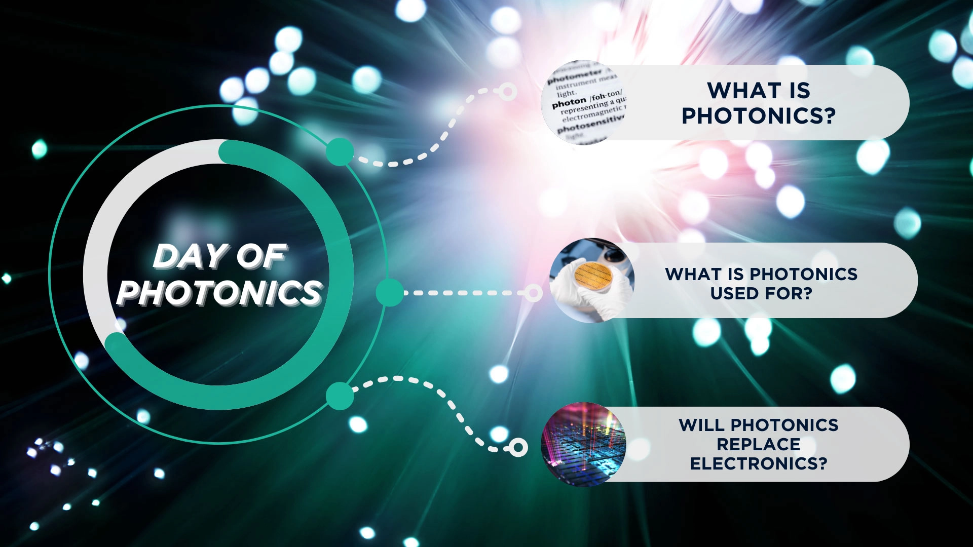
Photonics is the study and application of photon (light) generation, manipulation, and detection, often aiming to create, control, and sense light signals.
The term photonics emerged in the 60s and 70s with the development of the first semiconductor lasers and optical fibers. Its goals and even the name “photonics” are born from its analogy with electronics: photonics aims to generate, control, and sense photons (the particles of light) in similar ways to how electronics does with electrons (the particles of electricity).
Photonics can be applied in many ways. For the Day of Photonics, we will explore two categories:
Light is the fastest information carrier in the universe and can transmit this information while dissipating less heat and energy than electrical signals. Thus, photonics can dramatically increase the speed, reach, and flexibility of communication networks and cope with the ever-growing demand for more data. And it will do so at a lower energy cost, decreasing the Internet’s carbon footprint.
A classic example is optical fiber communications. The webpage you are reading was originally a stream of 0 and 1s that traveled through an optical fiber to reach you.
Outside of optical fibers, photonics can also deliver solutions beyond what traditional radio communications can offer. For example, optical transmission over the air could handle links between different sites of a mobile network, links between cars, or to a satellite out in space. At some point, we may even see the use of Li-Fi, a technology that replaces indoor Wi-Fi links with infrared light.
There are multiple sensing application markets, but their core technology is the same. They need a small device that sends out a known pulse of light, accurately detects how the light comes back, and calculates the properties of the environment from that information. It’s a simple but quite powerful concept.
This concept is already being used to implement LIDAR systems that help self-driving cars determine the location and distance of people and objects. However, there is also potential to use this concept in medical and agri-food applications, such as looking for undesired growths in the human eye or knowing how ripe an apple is.
No, each technology has its strengths.
When transmitting information from point A to B, photonics can do it faster and more efficiently than electronics. For example, optical fiber can transmit information at the speed of light and dissipate less heat than electric wires.
On the other hand, since electricity can be manipulated at the nanometer level more easily than light, electronics are usually better for building computers. There are some specific areas where photonic computers could outperform traditional electronic ones, especially given the rise of quantum computers that can be made with photonic components. However, most computer products will remain electronic for the foreseeable future.
Thus, photonics is not expected to replace electronics but to collaborate and integrate strongly with it. Most future applications will involve photonic systems transmitting or sensing information then processed by electronic computers.
Tags: DayofPhotonics2022, Integrated Photonics, Photonics Insights
July 11, 2023
Insights
July 11, 2023
In June 2022, transceiver developer II‐VI Incorporated (now Coherent Corp.) and optical networking solutions provider…
In June 2022, transceiver developer II‐VI Incorporated (now Coherent Corp.) and optical networking solutions provider ADVA announced the launch of the industry’s first 100ZR pluggable coherent transceiver. Discussions in the telecom sector about a future beyond 400G coherent technology have usually focused on 800G products, but there is increasing excitement about “downscaling” to 100G coherent products for certain applications in the network edge and business services. This article will discuss the market and technology forces that drive this change in discourse.
The 400ZR pluggables that have become mainstream in datacom applications are too expensive and power-hungry for the optical network edge. Therefore, operators are strongly interested in 100G pluggables that can house coherent optics in compact form factors, just like 400ZR pluggables do. The industry is labeling these pluggables as 100ZR.
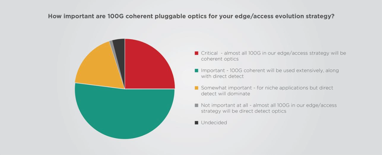
A recently released Heavy Reading survey revealed that over 75% of operators surveyed believe that 100G coherent pluggable optics will be used extensively in their edge and access evolution strategy. However, this interest had not really materialized into a 100ZR market because no affordable or power-efficient products were available. The most the industry could offer was 400ZR pluggables that were “powered-down” for 100G capacity.
With the recent II-VI Incorporated and ADVA announcement, the industry is showing its first attempts at a native 100ZR solution that can provide a true alternative to the powered-down 400ZR products. Some of the key specifications of this novel 100ZR solution include:
The 5 Watt-power requirement is a major reduction compared to the 15-Watt specification of 400ZR transceivers in the QSFP-DD form factor. Achieving this spec requires a digital signal processor (DSP) that is specifically optimized for the 100G transceiver.
Transceiver developers often source their DSP, laser, and optical engine from different suppliers, so all these chips are designed separately from each other. This setup reduces the time to market, simplifies the research and design processes, but comes with performance and power consumption trade-offs.
In such cases, the DSP is like a Swiss army knife: a jack of all trades designed for different kinds of optical engines but a master of none. DSPs co-designed and optimized for their specific optical engine and laser can significantly improve power efficiency. You can read more about co-design approaches in one of our previous articles.
Making 100ZR coherent optical transceivers more affordable is also a matter of volume production. As discussed in a previous article, if PIC production volumes can increase from a few thousand chips per year to a few million, the price per optical chip can decrease from thousands of Euros to mere tens of Euros. Such manufacturing scale demands a higher upfront investment, but the result is a more accessible product that more customers can purchase.
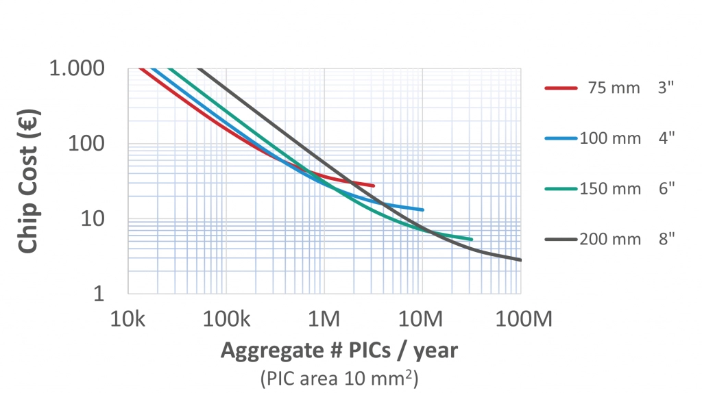
Achieving this production goal requires photonics manufacturing chains to learn from electronics and leverage existing electronics manufacturing processes and ecosystems. Furthermore, transceiver developers must look for trusted large-scale manufacturing partners to guarantee a secure and high-volume supply of chips and packages.
If you want to know more about how photonics developers can leverage electronic ecosystems and methods, we recommend you read our in-depth piece on the subject.
As the Heavy Reading survey showed, the interest in 100G coherent pluggable optics for edge/access applications is strong, and operators have identified use key use cases within their networks. In the past, there were no true 100ZR solutions that could address this interest, but the use of optimized DSPs and light sources, as well as high-volume manufacturing capabilities, can finally deliver a viable and affordable 100ZR product.
Tags: 100G coherent, 100ZR, DSP, DSPs, edge and access applications, EFFECT Photonics, Photonics Press Releases
June 23, 2023
Press Releases
June 23, 2023
– As a leading provider of highly integrated photonics solutions for optical communication products, EFFECT…
– As a leading provider of highly integrated photonics solutions for optical communication products, EFFECT Photonics has acquired the globally recognized ISO 9001 certification, reaffirming the high-quality standards it adheres to across its operations.
The company’s Brixham and Paignton sites were awarded the ISO 9001:2015 certification by the British Standards Institute (BSI). The scope of the certification covers the areas of design and development, including sales and marketing, and the manufacture and testing of products used in communication systems. ISO 9001 certifies that a management system, manufacturing process, service, or documentation procedure has all the requirements for standardization and quality assurance. Using ISO 9001 helps ensure that customers get consistent, good quality products and services.
Karen Whicker, Quality Manager, EFFECT PhotonicsThe ISO certification assures that EFFECT Photonics as a company has structure and the right systems in place. This offers our customers confidence that the company can produce products that meet their requirements because that is the ultimate goal of a quality system. It also expands our potential to venture into other segments, as it is valuable within various industries, such as the automotive and the medical
Acquiring the certification process began in 2020 by preparing all the necessary documentation and setting up the right systems for the review. In a two-step process, in April and September 2021, EFFECT Photonics received all the necessary approvals. Through this procedure, the company was able to showcase its vision, mission and values, which comprise its quality policy and its future objectives.
It is these professional systems that help us boost our credibility as a value player. There is an expectation from the end-customer point of view that we are certified for having these scalable systems and that they have been put in place for future growth. One of the things that we had to do for every process was put together a map. For each of the different business processes we have, there is a document that can guide you like a map so that you can see which systems we use, which documents, and which resources are applicable. It also explains how we measure the processes to see if they’re effective.
Karen Whicker, Quality Manager, EFFECT Photonics
Maintaining the certification, which lasts for three years, is an ongoing process, that involves frequent surveillance audits. Every three years the approval process is repeated and once the quality standards are assured, the certificate is reissued.
# # #
© 2026 EFFECT PHOTONICS All rights reserved. T&C of Website - T&C of Purchase - Privacy Policy - Cookie Policy - Supplier Code of Conduct